CIGS Nanomaterials for Electronics
Pearlhill Technologies has innovated CIGS nanoparticle semiconductor devices as advanced (1) phototransistors, (2) memristors, and (3) tunnel diodes. Pearlhill has fabricated our devices in collaboration with Professor Kris Campbell of Boise State University. The customer for the innovation and technology in this proposal are manufacturers of integrated circuits and devices for telecommunication and computers. Creating new telecommunication bandwidth will allow service provide service access to broadband applications for the end user, home or business, customers. Erbium-doped fiber amplifier (EDFA), multiplexer/demultiplexer, and optical networking solutions are a major asset to the majority of service providers in this industry. They allow the service providers to accommodate growth in bandwidth demand, extend the lifetime of existing fibers, improve profits by reducing operation and capital expenses. Raman Laser provide an optical output in the range of 1100-1700 nm, and EDFA in the 1535-1605 nm region with bandwidth of 35 nm. Freedom Photonics has provided validation for the new phototransistors that have optical input over the telecommunication to mid-infrared window, that is 1265-2400 nm. The CEO at Intel Corporation announced neuromorphic computing could unlock exponential gains in performance and power efficiency for artificial intelligence. Envisioned in 1971, the development of functional memristor is key to neuromorphic computing. Neuromorphic chips will enable smarter security cameras and smart-city infrastructure designed for real-time communication with autonomous vehicles, data analytics in medical imaging, automotive, transportation, defense, wearables, internet of things (IoT), and robotics sectors.
The Value Proposition: Raman Laser and EDFA are the two current products for optic-to-electricity conversion in the telecommunication window. The CIGS nanoparticles in this proposal detect light in the solar spectrum, that is, 250-2500 nm range, with bandwidth >35 nm. CIGS phototransistor will be developed to enable an extension of multiplexer/demultiplexer network links beyond 350 km in the state-of-the-art technology, without the need for amplifiers. With this development, CIGS phototransistors will be deployed in several products in terrestrial- and satellite-based free-space communication networks, and in communication systems for protection of electrical grids against radiation and electromagnetic pulses (EMPs). Several computer companies and institutions are seeking the capabilities of the ‘holy grail’ memristor for the development of the neuromorphic computer for advanced machine learning (ML), and artificial intelligence (AI). Pearlhill is working closely with Knowm, Inc, to develop cost competitive, optically gated memristor with ultra-low ‘dark’ noise, superfast two-way dynamic processing capacity, with three-order of memory density than the state-of-the-art products. Pearlhill targets as much as 50% reduction in the cost of production of the memristor.
Pearlhill and Freedom Photonics, in Santa Barbara, CA, have a collaboration for the development of custom nanomaterials for their circuit and device manufacturing business that is based on Indium-Phosphide (InP) and Gallium-Arsenide (GaAs), and Silicon-Germanium (SiGe) platforms. Freedom Photonics manufacture photonic components, modules and subsystems for high-performance fiber-, and free-space optical communication and sensing systems aimed at applications in diverse markets. They implement electronic control circuitry and system integration in a number of devices, and photonic integrated circuits, including, single frequency lasers, high-power, high-efficiency lasers, widely tunable lasers, photodetectors, semiconductor optical amplifiers, active and passive waveguide components, high speed modulators, mode converters, high speed switches, multiplexer/ demultiplexer, optical delay lines, and communication for protection of electric grids.
After recognizing huge benefits for our transformational phototransistor in the 1265-2400 nm telecommunication window, Pearlhill obtained a provisional patent (No. 62/761,106) for our technology, and discussed the innovation with Freedom Photonics, a leading manufacturer of circuits and devices. Based on their knowledge of the phototransistor segment, Dr. Daniel Renner, VP Business Development at Freedom photonics has stated that Pearlhill’s invention could revolutionize the playing field in the metro, long-haul and ultra-long-haul marketplaces. He stated that the optically gated transistors will provide a unique circuit isolation as well as optical-to-electrical coupling capability. He stated that, when fully developed, this technology could be a major game changer in the industry, and that Freedom Photonics would be interested in licensing it.
The Innovation: The innovation in this proposal is the development of optically-controlled transistors and memristors with superior responsivity, speed, low-power consumption, and designable spectral response range that can be integrated into a standard back-end-of-line CMOS process. These devices are unique and unconventional in that the optically-active material used is amorphous (a-Ge2Se3) when it is typically a crystalline material, and they do not require a separate gate electrode for the transistor. Without the requirement of a separate gate voltage, these devices can be switched directly by light, thus allowing light to completely control the operation of the switch. This is a significant improvement over the state-of-the-art phototransistors that require a gate voltage be applied prior to application of incident light.
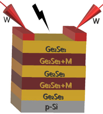
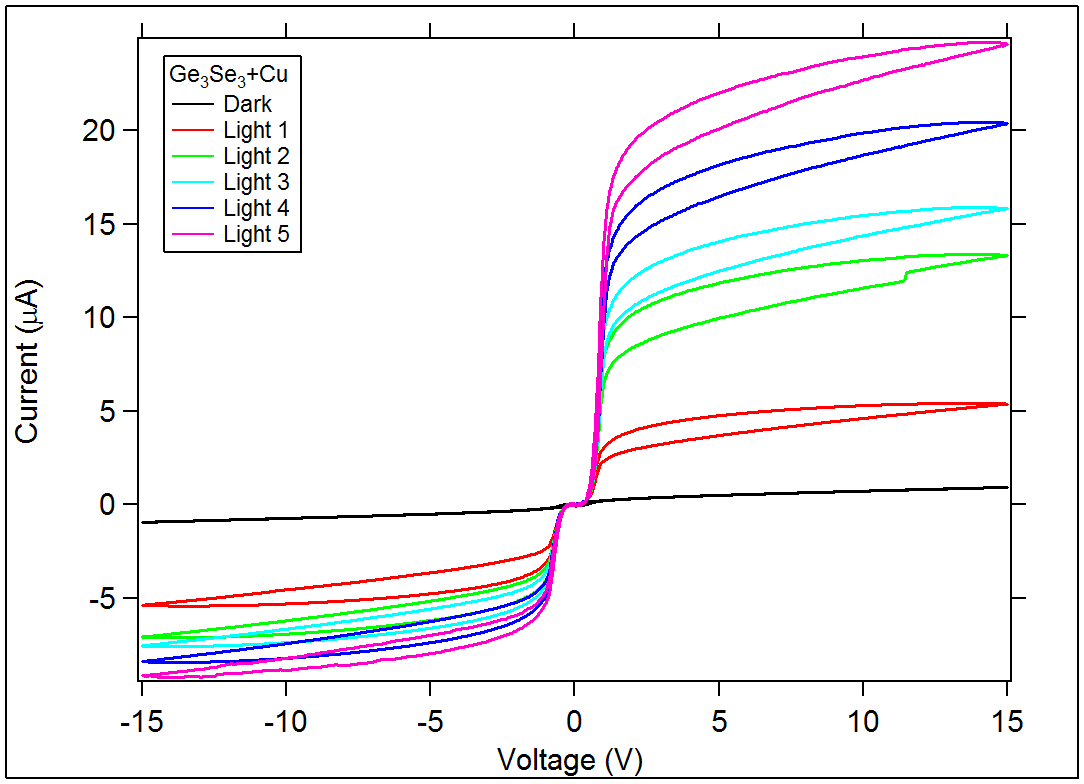
Our preliminary studies by Dr. Campbell at Boise State University (BSU) show that a two-terminal device with a layer of a-Ge2Se3 can exhibit a photo-response when illuminated. The device structure consists of 300 Å of a-Ge2Se3 sputtered on a p-Si (and to a lesser degree n-Si) substrate with a native oxide layer, and W electrodes on the a-Ge2Se3 layer. When a voltage is applied across the two W electrodes, I-V curves similar to a field effect transistor are obtained when light was incident on the sample (Fig. 1, top left graph). Addition of other elements (M = C, Sn, Ti, Cr, W, Cu, Al) to the device was performed through alternating layers of a-Ge2Se3 with cosputtered a-Ge2Se3–M (Fig. 2). The inclusion of these cosputtered alternating layers has been shown to alter the I-V response threshold voltage, curve shape, and responsivity, as well as incident light power and wavelength (Fig. 1). These additions also influence the switching speed of the device (Fig. 3). Addition of these elements has also led to the discovery of optically-controlled memristors. These include a-Ge2Se3–Cu which shows the memristive property of a pinched hysteresis loop when cycled with a periodic voltage input while under illumination (Fig. 4). The intensity of the current in the hysteresis loops is determined by the incident light intensity. Addition of these elements has also led to the discovery of optically-controlled memristors. These include a-Ge2Se3–Cu which shows the memristive property of a pinched hysteresis loop when cycled with a periodic voltage input while under illumination (Fig. 4). The intensity of thecurrent in the hysteresis loops is determined by the incident light.
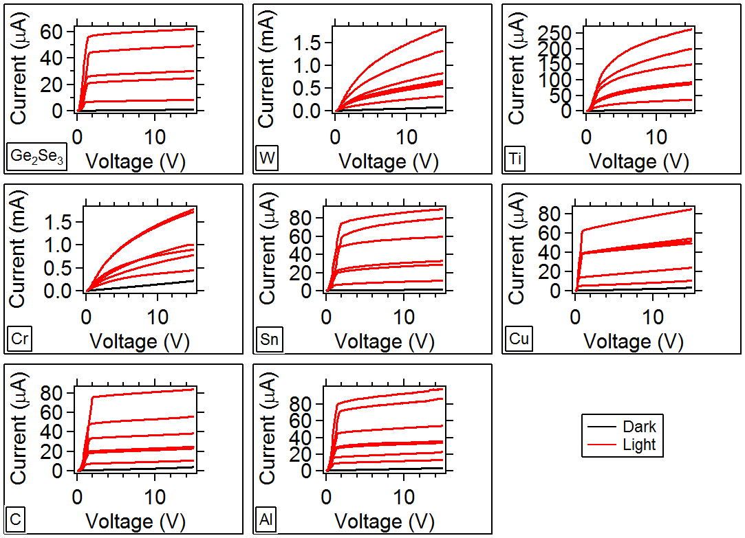
Based on these preliminary results, it appears promising that an a-Ge2Se3 phototransistor/memristor can potentially provide the basis for developing devices that are fast, tuned to a desired spectral region, low-power, and have high responsivity depending upon the dopant or nanoparticle included during fabrication. The mechanism of device operation is not fully understood, though a working hypothesis based on these preliminary results, indicates that addition of nanoparticles that are photon absorbers, such as CIGS, would provide additional photocurrent, speed, and spectral response tunability. In addition, it may be possible that some of the nanoparticles would act as quenchers and allow devices to switch off at a much faster rate. The nanoparticle location within the active layer may significantly influence device operation and will be part of the device development process.
Want to Know More?
Talk with one of the knowledgeable members of our team to see how we can help you achieve your goals.